1.3: Flash – Boot – Debug
Now that I have an executable bootstrap, I need to flash an actual board with it to check if it works as expected. On a member of the STM32F030 family, there are two options for flashing:
-
Use the Software Debug (SWD) interface with a ST-Link adapter and an utility software to flash.
-
Use the serial interface to communicate with the boot loader in System Memory via an USB to serial adapter.
As the bootstrap code I want to test does nothing except giving control to an idle loop, I will need extra debugging on top of the flashing functionality, so the SWD interface is a must for what I want to achieve here.
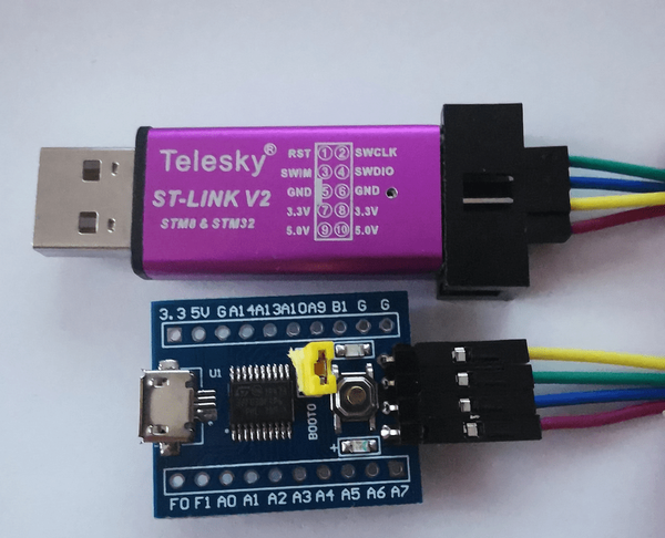
ST-Link
SWD interface
Arm Serial Wire Debug Port (SW-DP) is provided as a two wire interface. On the STM32F030, the functionality is activated at reset on two pins (PA13=SWCLK, PA14=SWDIO). Most boards available online have pre-soldered pins for Vcc=3.3V, Gnd, SWCLK and SWDIO.
ST-Link v2
ST-Link is an in-circuit debugger/programmer for the STM8 and STM32 chipsets. There are three versions of the product as well as mini versions. STM32 Discovery and Nucleo boards have an onboard ST-Link v2. I am using ST-Link v2 mini clones. For simple use cases, the ST-Link can provide power to the board to flash or test.

STM32 Cube Programmer
Referenced as STM32CubeProg on STMicroelectronics website, the STM32 Cube Programmer comes with USB drivers and a firmware upgrade utility for the ST-Link. It’s a java based application with available distribution for win32, win64 and Linux (v2.6.0 resolved the dependency issue to JRE when installing on Linux). There are regular updates to support the latest chipsets. I am currently using version v2.7.0.
Roadtesting the Bootstrap
First we activate the connection in the programmer.
  11:10:39 : STM32CubeProgrammer API v2.7.0
  11:10:57 : ST-LINK SN  : 55FF6B065177495619420887
  11:10:57 : ST-LINK FW  : V2J38S7
  11:10:57 : Board       : --
  11:10:57 : Voltage     : 3.28V
  11:10:57 : SWD freq    : 4000 KHz
  11:10:57 : Connect mode: Normal
  11:10:57 : Reset mode  : Software reset
  11:10:57 : Device ID   : 0x444
  11:10:57 : Revision ID : Rev 1.0
  11:11:00 : UPLOADING OPTION BYTES DATA ...
  11:11:00 :   Bank          : 0x00
  11:11:00 :   Address       : 0x1ffff800
  11:11:00 :   Size          : 16 Bytes
  11:11:00 : UPLOADING ...
  11:11:00 :   Size          : 1024 Bytes
  11:11:00 :   Address       : 0x8000000
  11:11:00 : Read progress:
  11:11:00 : Data read successfully
  11:11:00 : Time elapsed during the read operation is: 00:00:00.008
Then program and verify the bootstrap code. Either binary, Intel hex or Motorola S rec format are supported. Our Makefile as rules for binary and Intel hex, objcopy also support Motorola S record as an output format. Last build produced boot.hex.
  11:14:59 : Memory Programming ...
  11:14:59 : Opening and parsing file: boot.hex
  11:14:59 :   File          : boot.hex
  11:14:59 :   Size          : 10 Bytes
  11:14:59 :   Address       : 0x08000000
  11:14:59 : Erasing memory corresponding to segment 0:
  11:14:59 : Erasing internal memory sector 0
  11:14:59 : Download in Progress:
  11:14:59 : File download complete
  11:14:59 : Time elapsed during download operation: 00:00:00.123
  11:14:59 : Verifying ...
  11:14:59 : Read progress:
  11:14:59 : Download verified successfully
Finally check the registers in the MCU Core Panel:
MSP: 0x20001000
PC:  0x8000008
After reset, the stack pointer has been initialized and the program counter is on the idle loop under execution.
If we check the Programming Manual PM0215 STM32F0xxx Cortex-M0 programming manual, we can read the following about the registers MSP and PC:
Stack pointer (SP) register R13
In Thread mode, bit[1] of the CONTROL register indicates the stack
pointer to use:
● 0: Main Stack Pointer (MSP)(reset value). On reset, the processor
loads the MSP with the value from address 0x00000000.
● 1: Process Stack Pointer (PSP).

Program counter (PC) register R15
Contains the current program address. On reset, the processor loads the
PC with the value of the reset vector, which is at address 0x00000004.
Bit[0] of the value is loaded into the EPSR T-bit at reset and must be
1.
-
According to this, initial values for MSP and PC registers are fetched from address 0x00000000 and 0x00000004 respectively, but we have located our isr table at the beginning of the Flash memory at address 0x08000000! This works because the memory space at address 0 is a mirror of another memory area. Which area is mirrored depends of the state of the BOOT0 pin. On the board I am testing, there is a jumper to select either Flash or System memory by setting the state of the BOOT0 pin to high or low.
-
The ESPR T-bit, mentioned in the description of the PC register is the Thumb bit. As I highlighted before when we checked the output of our first build, bit 0 of the second entry in our isr table is set to 1 as requested by this specification.
Checkpoint
We have used the Serial Wire Debug (SWD) interface to flash and debug our bootstrap in an actual board using a ST-Link hardware adapter and STM32 Cube Programmer application.
Next I will provide feedback of execution directly through the board.
© 2020-2021 Renaud Fivet